- Overview
- Product Description
- Detailed Photos
- Product Parameters
- Process Flow
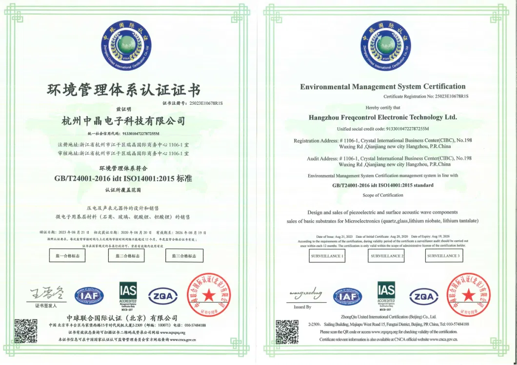
- Certifications
- Packaging & Shipping
- Our Advantages
Basic Info.
Product Description
The LiNbO 3: Fe: Mn double doped LiNbO 3: Fe: Mn was prepared by doping Fe and CE into LiNbO 3 crystal.
By using the photorefractive, electro-optic and birefringence effects of LiNbO 3 crystal, the self enhancement effect in the nonvolatile holographic recording of double doped LiNbO 3: Fe: Mn crystal can effectively improve the photorefractive sensitivity of the crystal to red light. The micro optical components and optical systems designed and fabricated in a single crystal have many advantages, such as multi-function, integration and anti-interference, which are the research directions with important application prospects. Among them, the core technology is to fabricate high-efficiency nonvolatile holographic grating in a single lithium Niobate crystal.


| Material | Optical Grade LiNbO3 wafes doped with Fe / Mn | |
| Curie Temp | 1142±2.0ºC | |
| Cutting Angle | X/Y/Z etc | |
| Diameter/size | 2"/3"/4"/6" | |
| Tol(±) | <0.20 mm | |
| Thickness | 0.18 ~ 0.5mm or more | |
| Primary Flat | 16mm/22mm /32mm | |
| TTV | <3µm | |
| Bow | -30<bow<30 | |
| Warp | <40µm | |
| Orientation Flat | All available | |
| Surface Type | Single Side Polished /Double Sides Polished | |
| Polished side Ra | <0.5nm | |
| S/D | 20/10 | |
| Edge Criteria | R=0.2mm or Bullnose | |
| Optical doped | Fe/Zn/MgO etc for optical grade LN< wafers | |
| Wafer Surface Criteria | Refractive index | No=2.2878/Ne=2.2033 @632nm wavelength |
| Contamination, | None | |
| Particles ¢>0.3 µ m | <= 30 | |
| Scratch , Chipping | None | |
| Defect | No edge cracks, scratches, saw marks, stains | |
| Packaging | Qty/Wafer box | 25pcs per box |
Application list:
Integrated waveguide photonics; Wave Guide Lasers; Quasi-phase Matching for SHG&OPO; EO waveguide Phase & Amplitude Modulators
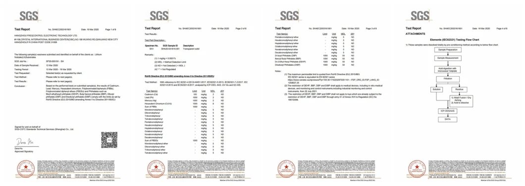
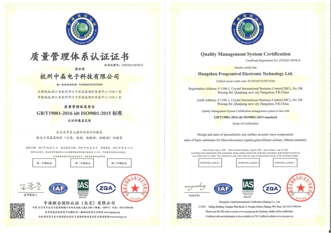


CQT's primary goal is "To be a reliable primary microelectronics substrates supplier in today's World". The entire organization, beginning with top management, has worked consistently to meet this goal.
Our reputation for quality is based on a commitment to the newest and most effective design, manufacturing, testing, and management procedures - including, but not limited to, design for manufacturing, statistical process control, lean manufacturing, and continuous improvement methodologies. We have had a fully implemented and effective IATF16949 Quality Management System.
CQT is committed to conduct its all operations in a socially responsible, ethical, and sustainable manner to protect the environment and ensure the safety and health of our employees, customers, and surrounding communities. We are also committed to continuous improvement on all environmental issues. CQT maintains ISO9001/ISO14001 certifications and also implements the EICC standards. and implemented the Electrical Industry Code of Conduct as well.
